Effective engineering of materials defects and defect properties on the atomic scale is crucial for creating materials for applications in nanotechnology, i.e., ultra-miniaturization of sensors, storage, processing, and communication. Silicon carbide (SiC) is a large bandgap semiconductor that is in focus for its potential for applications in quantum information processing. It appears possible to engineer defects in SiC with optical and spin properties that are suitable as single photon sources, and states with long enough lifetime to act as qubit memory. We have automated the setup of ab-inito calculations for several forms of point defects (impurities, interstitials, vacancies, and their complexes.) We are using this to perform a systematic large-scale computational study to enumerate a wide range of point defect properties, in particular, photoluminescence lines. The resulting database of predicted defect properties will be used for identifying defects that appear in experiments, explain their physics, and find out how to engineer them with desired properties to target nanotechnology applications. We are also working on extending the automated tools to other host materials.
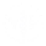
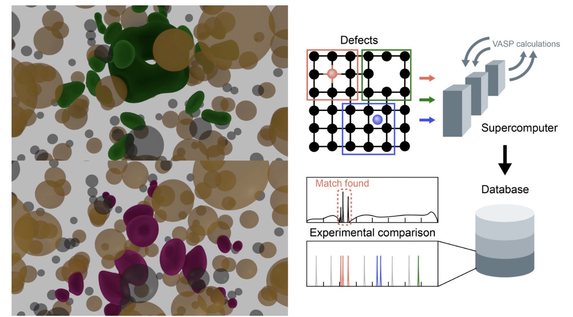
Fig: Left: Electron orbitals in a defect in SiC with Si (brown) and C (black) atoms, the ground electron state (purple) and a state where the electron has been exited by a photon (green). Right: A schematic of the high-throughput scheme used for building a database of defect data to use for identification of unknown defects and predict their properties.
Video: https://d.pr/GKmKFW
Ref: First principles predictions of magneto-optical data for semiconductor point defect identification: the case of divacancy defects in 4H–Si, Joel Davidsson, Viktor Ivády, Rickard Armiento, N. T. Son, Adam Gali, and Igor A. Abrikosov, New J. Phys. 20, 023035 (2018).